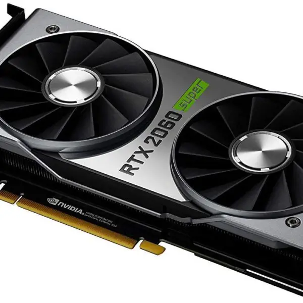
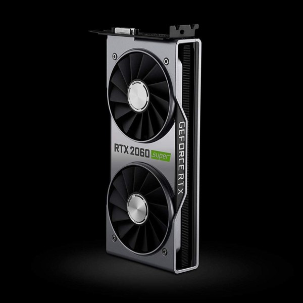
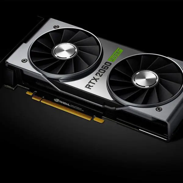
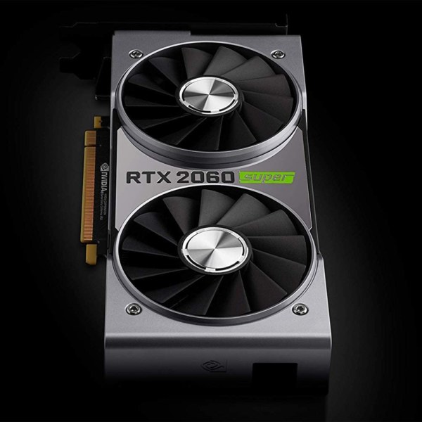
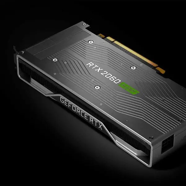
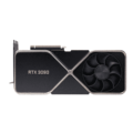
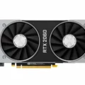
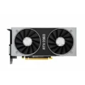
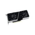
Nvidia GeForce RTX 2060 SUPER 8GB
-
Cores: 2176 CUDA CORES
-
Base Clock: 1470 MHz
-
Boost Clock: 1650 MHz
-
Memory: 8GB GDDR6
-
VR Ready: YES
-
Resolutions Supported: 7680x4320
Nvidia GeForce RTX 2060 SUPER Features
The Nvidia GeForce RTX 2060 SUPER 8GB features Turing 12nm architecture with 2176 CUDA Cores. It has a base clock of 1470 MHz as well as a boost clock of 1650 MHz. There are 10.8 Billion transistors, 136 Texture Units and additionally 64 ROPs. The memory powering this card is 8 GB of GDDR6 memory. This clocked at 14000 MHz effective. The memory interface width is 256-bit and it has a memory bandwidth of 448 GB/s.
In terms of technologies on this card, there is DirectX 12, G-Sync, Open CL 1.2, OpenGL 4.6 and also Shader Model 6.5. This card is VR Ready according to Nvidia. Furthermore, there are extra technologies which include Ray Tracing Cores, Tensor Cores, NVIDIA DLSS, NVIDIA Adaptive Shading, Real-Time Ray Tracing, NVIDIA GeForce Experience, NVIDIA Ansel, NVIDIA Highlights, Game Ready Drivers, Microsoft DirectX 12 Ultimate, Vulkan API, HDCP 2.2, NVIDIA GPU Boost, Designed for USB Type-C and VirtualLink as well as NVIDIA Encoder (NVENC) (Turing).
The maximum digital resolution of the Nvidia GeForce RTX 2060 SUPER 8GB is 7680×4320. This can be done with the I/O included which are DisplayPort 1.4a, HDMI 2.0b, DL-DVI-D and also USB-C. This card does not feature any single link DVI or VGA ports.
To power this card you need 1 x 8 pin connector available. This is because the graphics card has a TGP of 175 W which requires a recommended 550 W power supply. This card comes in at 4.435” (112.6mm) x 9.0” (228.60mm) x 2-Slot. When released, on the 9th July 2019, the card retailed at $399 USD.
Check Nvidia GeForce RTX 2060 SUPER 8GB variants here.
Specifications
Purchase This Card
| Amazon | View Price At Amazon |
General
| Manufacturer | Nvidia |
| Type | Desktop |
| Series | GeForce 20 |
| Variant | RTX 2060 Super |
| GPU Architecture | Turing |
| Code Name | TU106-410-A1 |
| Fabrication Process | TSMC 12nm |
| Die Size | 445 mm² |
| Base Clock | 1470 MHz |
| Boost Clock | 1650 MHz |
| Transistor Amount | 10.8 Billion |
Cores & Texture Config
| Cores | 2176 CUDA CORES |
| Texture Units | 136 |
| ROPs | 64 |
| Ray Tracing Cores | 34 |
| Tensor Cores | 272 |
| Compute Units | - |
| L2 Cache | 4MB |
| Infinity Cache | - |
Memory
| Memory Size | 8GB |
| Memory Type | GDDR6 |
| Memory Clock | 1750 MHz |
| Memory Clock Effective | 14 Gbps |
| Memory Interface Width | 256-bit |
| Memory Bandwidth | 448 GB/s |
Performance
| Half Precision FP16 | 14.3616 TFLOPS |
| Single Precision FP32 | 7.1808 TFLOPS |
| Double Precision FP64 | 0.2244 TFLOPS |
Floating Point Operations Per Clock Cycle
| Half Precision FP16 | 4 |
| Single Precision FP32 | 2 |
| Double Precision FP64 | 1/16 |
Fillrate
| Texture (GT/s) | 224.4 |
| Pixel (GP/s) | 105.6 |
Technologies
| DirectX® Version | 12 |
| G-Sync/FreeSync | |
| OpenCL | 1.2 |
| OpenGL | 4.6 |
| Shader Model | 6.5 |
| Vulkan | 1.3 |
| SLI/Crossfire Ready | |
| VR Ready | |
| RGB Lighting | |
| Extra Technologies | Ray Tracing Cores, Tensor Cores, NVIDIA DLSS, NVIDIA Adaptive Shading, NVIDIA GeForce Experience, NVIDIA Ansel, NVIDIA Highlights, Game Ready Drivers, Microsoft DirectX 12 Ultimate, Vulkan API, HDCP 2.2, NVIDIA GPU Boost, Designed for USB Type-C and VirtualLink, NVIDIA Encoder (NVENC) (Turing) |
Connectivity
| Maximum resolution | 7680x4320 |
| Max HDMI Resolution | 3840x2160 @ 60 Hz |
| Max DP Resolution | 7680x4320 @ 120 Hz |
| Display Port | 1.4a x3 |
| HDMI | 2.0b x1 |
| USB-C | USB-C VirtualLink x1 |
| Dual Link DVI | DVI-D x1 |
| Single Link DVI | No |
| VGA | No |
Requirements
| Interface | PCI-E 3.0 x16 |
| Power Connectors | 1 x 8 pin |
| PSU Recommendation | 550 W |
| Graphics Card Power | 175 W |
Dimensions
| Length | 4.435” (112.6mm) |
| Width | 9.0” (228.60mm) |
| Height | 1.4" (35.5mm) |
| Slot Width | 2 Slot |
Extra Information
| Price (at release) | $399 USD |
| Weight | 1kg |
| Released | 09 July, 2019 |
Offers


Price History
Price History for ASUS ROG Strix GeForce RTX 2060 Super Advanced Overclocked EVO 8G GDDR6 HDMI DisplayPort USB...
Statistics
| Current Price | $645.00 | May 13, 2025 |
| Highest Price | $645.00 | February 27, 2025 |
| Lowest Price | $547.07 | October 15, 2024 |
Last price changes
| $645.00 | February 27, 2025 |
| $548.01 | February 25, 2025 |
| $547.07 | October 15, 2024 |
| $547.99 | September 18, 2024 |
| $548.00 | September 16, 2024 |

Reviews
Videos
Disclaimer Note
The information provided is for reference only and may not be 100% accurate
More Graphics Cards From Nvidia


Comments
Recently Added

Best Selling Graphics Cards


